Advantages:
- Smaller components.
- Much higher component density (components per unit area) and many more connections per component.
- Components can be placed on both sides of the circuit board.
- Higher density of connections because holes do not block routing space on inner layers, nor on back-side layers if components are mounted on only one side of the PCB.
- Small errors in component placement are corrected automatically as the surface tension of molten solder pulls components into alignment with solder pads. (On the other hand, through-hole components cannot be slightly misaligned, because once the leads are through the holes, the components are fully aligned and cannot move laterally out of alignment.)
- Better mechanical performance under shock and vibration conditions (partly due to lower mass, and partly due to less cantilevering)
- Lower resistance and inductance at the connection; consequently, fewer unwanted RF signal effects and better and more predictable high-frequency performance.
- Better EMC performance (lower radiated emissions) due to the smaller radiation loop area (because of the smaller package) and the lesser lead inductance.[16]
- Fewer holes need to be drilled. (Drilling PCBs is time-consuming and expensive.)
- Lower initial cost and time of setting up for mass production, using automated equipment.
- Simpler and faster automated assembly. Some placement machines are capable of placing more than 136,000 components per hour.
- Many SMT parts cost less than equivalent through-hole parts.Smaller components.
- Much higher component density (components per unit area) and many more connections per component.
- Components can be placed on both sides of the circuit board.
- Higher density of connections because holes do not block routing space on inner layers, nor on back-side layers if components are mounted on only one side of the PCB.
- Small errors in component placement are corrected automatically as the surface tension of molten solder pulls components into alignment with solder pads. (On the other hand, through-hole components cannot be slightly misaligned, because once the leads are through the holes, the components are fully aligned and cannot move laterally out of alignment.)
- Better mechanical performance under shock and vibration conditions (partly due to lower mass, and partly due to less cantilevering)
- Lower resistance and inductance at the connection; consequently, fewer unwanted RF signal effects and better and more predictable high-frequency performance.
- Better EMC performance (lower radiated emissions) due to the smaller radiation loop area (because of the smaller package) and the lesser lead inductance.[16]
- Fewer holes need to be drilled. (Drilling PCBs is time-consuming and expensive.)
- Lower initial cost and time of setting up for mass production, using automated equipment.
- Simpler and faster automated assembly. Some placement machines are capable of placing more than 136,000 components per hour.
- Many SMT parts cost less than equivalent through-hole parts.

Features:
- Product Name: PCB Assembly Service
- Surface Mount Assembly
- Solder Mask: Green, Blue, White, Black, Etc.
- Min. Hole Size: 0.1mm
- PCB Thickness: 0.2mm - 10.0mm
- Material: FR-4, FR-4 High Tg, Rogers, Etc.
- Copper Thickness: 0.5OZ - 12OZ
- Soldering and Assembly Service
- PCB Manufacturing Service
Technical Parameters:
| Parameter |
Specification |
| PCB Thickness |
0.2mm - 10.0mm |
| PCB Layer |
2-68 Layers |
| Min. Line Spacing/Width |
2.5mil / 2.5mil |
| Copper Thickness |
0.5OZ - 12OZ |
| Solder Mask |
Green, Blue, White, Black, Etc. |
| Testing |
AOI, X-Ray, Flying Probe, Etc. |
| Min. Hole Size |
0.1mm |
| Silk Screen |
White, Black, Yellow, Etc. |
| Product Type |
PCB Assembly Service |
| PCB Size |
Max 610mm * 1200mm |
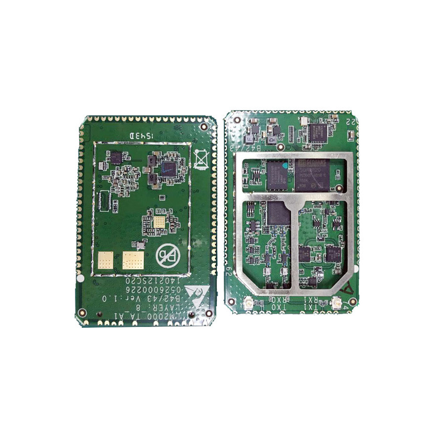
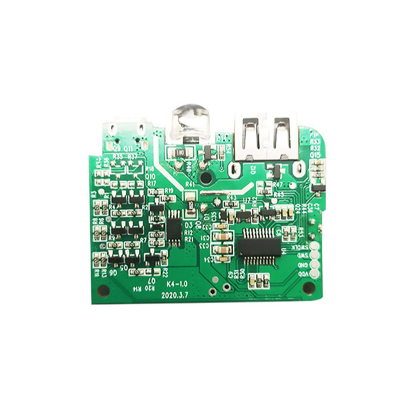
| Printed Circuit Board Assembly |
Surface Mount Assembly, Through-Hole Assembly, Mixed Assembly, BGA Assembly |
Customization:
PCB Assembly Service
Brand Name: Cesgate
Model Number: NA
Place of Origin: China
Certification: UL, IATF16949, ISO9001, ISO14001
Minimum Order Quantity: 1PCS( NO MOQ)
Price: $1.00
Packaging Details: PCB: Vacuum Packing / PCBA: ESD + vacuum Packing
Delivery Time: 3-7 working days
Payment Terms: T/T, L/C
Supply Ability: 13kk soldering spot/day
Customized Service of Printed Circuit Board Assembly (PCBA)
Solder Mask: Green, Blue, White, Black, Etc.
PCB Layer: 2-68 Layers
Silk Screen: White, Black, Yellow, Etc.
Min. Hole Size: 0.1mm
Surface Finish: HASL, ENIG, OSP, Etc.
Cesgate offers a custom and comprehensive Printed Circuit Board Assembly (PCBA) service that meets the highest standards of quality and reliability. With our professional engineers, advanced manufacturing facilities, strict quality control, and competitive prices, we guarantee the highest quality and performance of PCB assembly services for customers around the world.
We provide a complete solution for all your PCB assembly needs. From design to assembly, we can handle all aspects of your project. We can also provide custom services such as prototyping, design verification and testing, to ensure that your product is of the highest quality.
We value customer satisfaction and are committed to providing the highest quality services to meet your needs. Contact us today to learn more about our PCB assembly services and how we can help you with your project.
Support and Services:
PCB Assembly Service Technical Support and Service
Provide professional technical support and service for PCB Assembly Service. We have a team of experienced engineers and technicians who are dedicated to providing high-quality service. Our service includes:
- Design consultation and review
- Component sourcing and procurement
- Testing and inspection
- On-time delivery
- Warranty repair and maintenance
We have been in the industry for many years and are committed to providing our customers with the best service possible. If you have any questions or concerns, please feel free to contact us. We are here to help.
Packing and Shipping:
PCB Assembly Service Packaging and Shipping:
We package and ship our PCB Assembly Service products according to industry standards. We use high-quality packaging materials to ensure safe delivery of all products. We use a variety of shipping methods, including airfreight, ground transportation, and express services. We also provide tracking information to ensure that your package arrives at its destination on time.
FAQ:
Q: How long is the shelf life of the PCB board and how should it be stored?
CESGATE: 25℃ / 60%RH is recommended when the PCB is stored. The plate itself has no shelf life, but if it exceeds three months, it needs to be baked to remove moisture and stress, and it should be used immediately after baking. It is recommended that the pieces should be loaded within 6 months of storage to reduce the phenomenon of rejection and explosion.
Q: What is your delivery date?
CESGATE: The general sample delivery time is 6 working days for single and double-sided boards, 7 working days for 4-layer boards, and an additional working day for every 2 layers. However, if there are special processes, additional working days will be added according to the situation.
Generally, the delivery time for mass production is 10 working days for single and double-sided panels, and 15 working days for multi-layer panels. However, if there is a special process or more than a certain number of working days, the working days will be additionally increased according to the situation; you can also pay the urgent fee to shorten the number of days, please contact Contact the business specially proposed, depending on the individual situation to provide expedited days.
Q: What are the types of solder mask?
CESGATE: There are traditional epoxy resin IR baking type, UV curing type, Liquid Photo Imageable Solder Mask and Dry film solder mask. Currently, the liquid solder mask is the main type.Q: What are the types of solder mask?
CESGATE: There are traditional epoxy resin IR baking type, UV curing type, Liquid Photo Imageable Solder Mask and Dry film solder mask. Currently, the liquid solder mask is the main type.